D. McNerny, B, Viswanath, D. Copic, F. Laye, C. Prohoda, A. Brieland-Shoultz, E.S. Polsen, N.T. Dee, V.S. Veerasamy, A.J. Hart. Direct fabrication of graphene on SiO2via thin film stress engineering.Scientific Reports, (4):5049, 2014. [http://dx.doi.org/10.1038/srep05049] [MIT News]
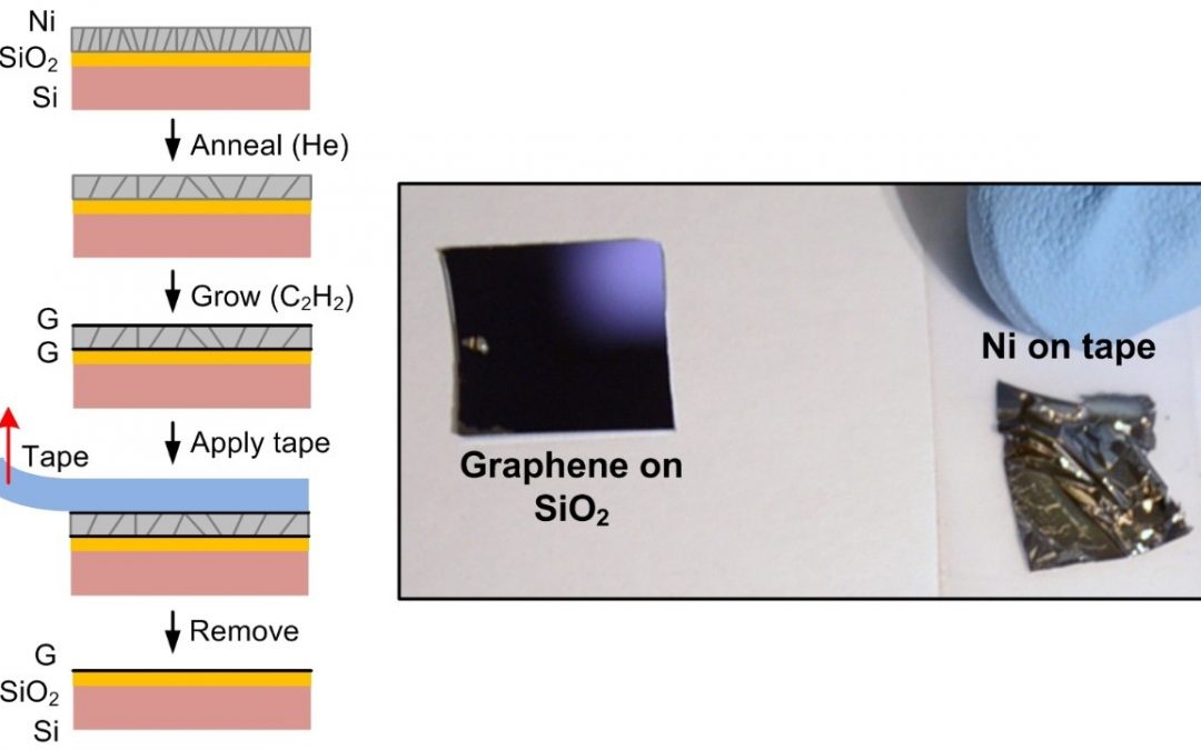
We demonstrate direct production of graphene on SiO2 by CVD growth of graphene at the interface between a Ni film and the SiO2 substrate, followed by dry mechanical delamination of the Ni using adhesive tape. This result is enabled by understanding of the competition between stress evolution and microstructure development upon annealing of the Ni prior to the graphene growth step. When the Ni film remains adherent after graphene growth, the balance between residual stress and adhesion governs the ability to mechanically remove the Ni after the CVD process. In this study the graphene on SiO2 comprises micron-scale domains, ranging from monolayer to multilayer. The graphene has >90% coverage across centimeter-scale dimensions, limited by the size of our CVD chamber. Further engineering of the Ni film microstructure and stress state could enable manufacturing of highly uniform interfacial graphene followed by clean mechanical delamination over practically indefinite dimensions. Moreover, our findings suggest that preferential adhesion can enable production of 2-D materials directly on application-relevant substrates. This is attractive compared to transfer methods, which can cause mechanical damage and leave residues behind.